Amy’s work to fabricate a fully bottom-up metal-oxide-semiconductor (MOS) gate stack is now published in Applied Physics Letters. She combined our SCALES patterning technique and atomic layer deposition (ALD) to achieve a gate stack that is self-aligned with the underlying silicon doping profile. Great work!
Prof. Filler visits NYU and NCSU
Prof. Filler visited the Departments of Chemical and Biomolecular Engineering at New York University and North Carolina State University in recent weeks. Thank you to Profs. Ayaskanta Sahu and Greg Parsons for their respective invitations and hospitality!
Congratulations to Amar and Maritza
A hearty congratulations to Amar Mohabir and Maritza Mujica for successfully defending their theses! They have accepted positions at Lam Research and ASM, respectively. We wish you all the best in these new roles.
Prof. Filler presents a series of virtual talks
Prof. Filler recently presented virtual seminars at Stanford University and Oklahoma State University. In addition, he gave invited talks at the 2020 Spring/Fall MRS Meeting and Lorentz Center Workshop on Nanomaterial Formation at Fluid-Fluid Interfaces. Thank you to all the hosts and conference organizers for these wonderful opportunities!
Welcome Daniel Aziz
We are delighted to welcome Ph.D. student Daniel Aziz to the lab. His project will focus on the development of bottom-up patterning and deposition techniques for semiconductor nanowires. He received his B.S. in Chemical Engineering from the University of Florida. Welcome!
Fundamental Manufacturing Process Innovation Changes the World
An updated version of the piece written by Profs. Filler and Realff on process innovation is now available on Medium.

Maritza's manuscript accepted to ACS Applied Nano Materials
Maritza Mujica was lead author on a manuscript titled “The Geode Process: Hollow Silica Microcapsules as a High Surface Area Substrate for Semiconductor Nanowire Growth” that was recently accepted to ACS Applied Nano Materials. The Geode process is inspired by the geological rock formation of the same name. Hollow silica microcapsules lined with the metal nanoparticles that seed nanowire growth are first produced with a scalable emulsion templating technique. A dried microcapsule powder is then loaded into a chemical vapor deposition reactor where it provides a surface area for nanowire growth several orders of magnitude larger than would be possible on conventional, flat substrates. Congrats to Maritza and all her co-authors on this initial demonstration!

Amar's manuscript accepted to ACS Nano
Amar’s manuscript titled “Bottom-Up Masking of Si/Ge Surfaces and Nanowire Heterostructures via Surface Initiated Polymerization and Selective Etching” has been accepted to ACS Nano! In this work, Amar combines ideas from nanowire growth, surface chemistry, and polymer science to demonstrate a new method to pattern the surface of semiconductor nanowires. Congrats!

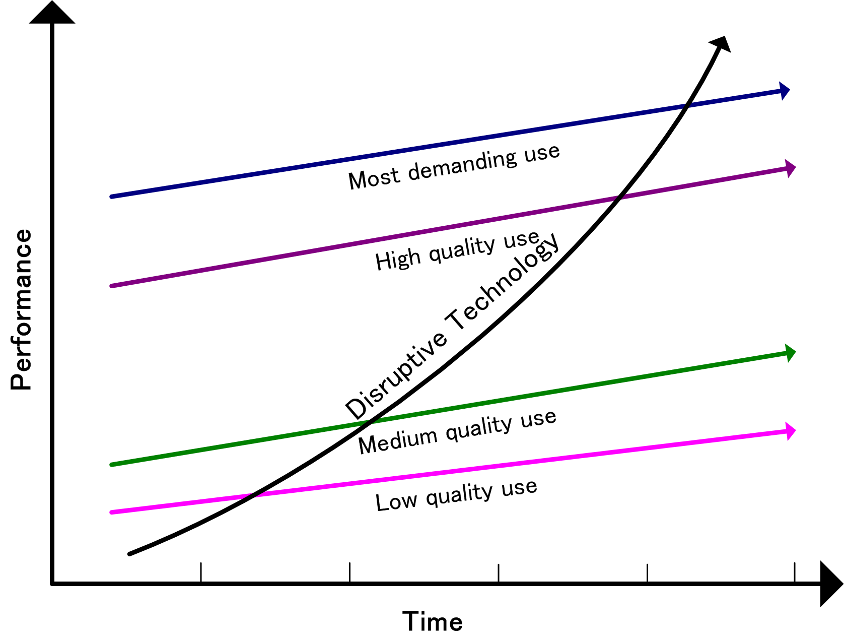
Busting process innovation myths
Drs. Filler and Realff just published a perspective titled Technological Innovation Hiding in Plain Sight: How Manufacturing Processes Transform Society without Leaving a Trace.
They take an intentionally revisionist approach to show that many technological innovations are more ‘process’ than is generally appreciated.
The document is meant to be a starting point, one that initiates a dialogue among scientists, technologists, funders, and policymakers about the value of such innovations and how they can best be nurtured in the future.

Dr. Filler on the Sustainable Nano podcast
Dr. Filler joined host Miriam Krause on the Sustainable Nano podcast to talk about “hyper-scaling” electronics manufacturing. Check it out!

Trey wins 1st place!
Mackey (Trey) Long, one of our two summer interns, won 1st place for his final presentation as part of the SURE program. Congratulations!

Filler Lab publishes with researchers from Aachen University in ACS Photonics
Collaborative work with the labs of Matthias Wuttig and Thomas Taubner at Aachen University was just published in ACS Photonics. The paper, titled “Quantification of carrier density gradients along axially-doped silicon nanowires using infrared nanoscopy,” demonstrates a route to measure dopant gradients in Si nanowires. The nanowires used in this study were synthesized by Dmitriy Boyuk and Amar Mohabir.
Maritza and Amar present at the ACS Colloid and Surface Science Symposium
Maritza Mujica and Amar Mohabir proudly presented their latest work at the ACS Colloid and Surface Science Symposium, which was held June 16-19, 2019 at Georgia Tech.

Prof. Filler visits AFRL
Prof. Filler visited the Materials and Manufacturing Directorate at the Air Force Research Lab (AFRL) in Dayton, OH on May 17th, 2019. He visit with lab scientists and presented a talk titled “Transistor Inks for Additive and Scalable Electronics: A Story of Process Innovation.” Thanks to Chris Tabor for hosting his visit!
Prof. Filler visits Vanderbilt, UC Boulder, and ALD NanoSolutions
Prof. Filler visited with the students and faculty at Vanderbilt University on March 24, 2019 where he spoke about “Nanoscale Programming of Semiconductors.” Thanks to Prof. Piran Kidambi for hosting!
On April 7th, 2019, Prof. Filler visited the University of Colorado - Boulder to present a talk titled “The Functionality-Scale Nexus.” A very special thanks to Prof. Steve George for the opportunity to visit!
Prof. Filler made one final stop at ALD NanoSolutions on April 8th.
Eric Tervo and Michael Gustafson publish in Applied Physics Letters
Eric Tervo and Michael Gustafson’s paper titled “Photonic thermal conduction by infrared plasmonic resonators in semiconductor nanowires” has been published in Applied Physics Letters. They model the thermal excitation and waveguiding of photons inside in dopant-engineered semiconductor nanowires, showing that photons promise to carry as much heat as phonons and electrons. Their results identify a new mode of heat transport inside solids, suggest experiments to definitively demonstrate this effect, and open the door to solid-state thermal switches.

GT-Rutgers team publishes in Small
A collaborative team from the Filler Lab at Georgia Tech and the Shan Lab at Rutgers University just published a paper titled “Contactless Electrical and Structural Characterization of Semiconductor Nanowires with Axially Modulated Doping Profiles” in the journal Small. The works demonstrates a route to determine the electrical conductivities of nanowires containing two differently doped regions in a high-throughput, non-contact manner. It sets the stage for characterizing complete electronic devices, which similarly consist of multiple types of domains.
Prof. Filler talks at the SEMI Flex conference and visits HP Labs
Prof. Filler presented at the SEMI Flex conference in Monterey, CA and also visited HP Labs in Palo Alto, CA.
Welcome to Sampath Kommandur and Thang Pham!
Sampath Kommandur and Thang Pham have joined the lab as postdocs to work on new types of nanowire growth. Sampath received his Ph.D. from Georgia Tech where he focused on advanced thermal metrology techniques. Thang received his Ph.D. from UC Berkeley where he specialized in the electron microscopy characterization of 1-D nanomaterials. Welcome!
Prof. Filler talks tech innovation on WREK's Lost in the Stacks
Prof. Filler joined the hosts of WREK’s Lost in the Stacks to talk about technological innovation and Clay Christensen’s The Innovator’s Dilemma. Check it out!